

















JDM

IADIY provides end-to-end Joint Design Manufacturing (JDM) across vision, laser sensing, optics, edge computing, and low-power display. With agile Taiwan-based R&D, strict NDA protection, and multi-region supply chain flexibility, we help global hardware innovators overcome engineering bottlenecks and accelerate time-to-market.
Traditional hardware programs often stall due to rigid off-the-shelf specs, multi-vendor finger-pointing, or opaque supply chains. IADIY engineers backward from your real-world deployment scenario to eliminate friction from prototype to volume.
| Criteria | Single-Category Vendors | Tier-1 ODMs / Contract Manufacturers | IADIY Collaborative JDM |
|---|---|---|---|
| Product Scope | Specializes in only one domain (camera, laser, e-paper, or IPC) | Broad catalog, mostly rigid high-volume reference platforms | 5 integrated lines: Vision, Laser, Optics, Embedded & E-Paper |
| System Integration | Customer must source and integrate multiple vendors independently | Capable, but locked into proprietary house platforms | Cross-module co-engineering into a turnkey working system |
| Design Ownership | Limited to minor modifications of existing SKUs | Manufacturer-led design; identical platforms sold to competitors | Joint specification definition and collaborative architecture |
| IP Ownership | Varies by vendor policy | Typically retained by the manufacturer | Flexible & negotiable—clearly defined prior to project kickoff |
| Entry Barrier | Requires formal sample qualification or eval-kit applications | High MOQ focus with lengthy upfront commercial vetting | Immediate off-the-shelf store samples for rapid POC validation |
Breaking down traditional hardware development silos. IADIY structures optical micro-structures, laser metrology, custom compute carrier boards, and display interfaces into a cohesive three-tier architecture built for demanding environments.
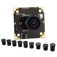
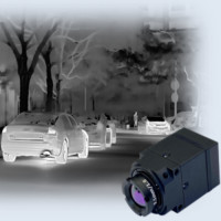
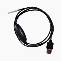
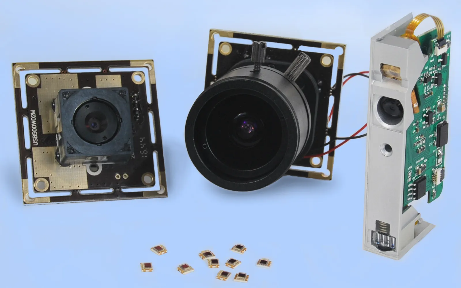
MIPI, USB, and FPC miniature HD cameras, ultra-low-light thermal night vision, and medical endoscope optics.
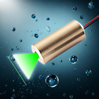
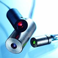
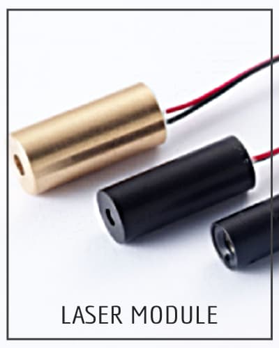
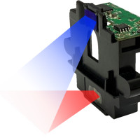
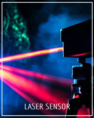
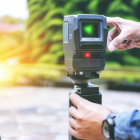
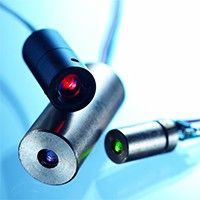
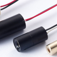
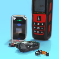
RGB and IR line lasers, solid-state LiDAR, and millimeter-precision Time-of-Flight (ToF) distance sensors.
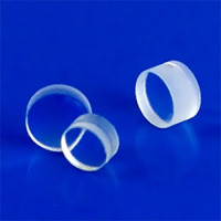
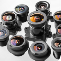
Custom molded glass aspherical lenses, high-precision collimators, narrow-bandpass filters, and sub-micron AR coatings.
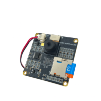
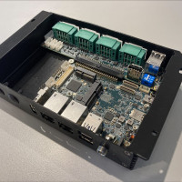
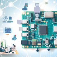
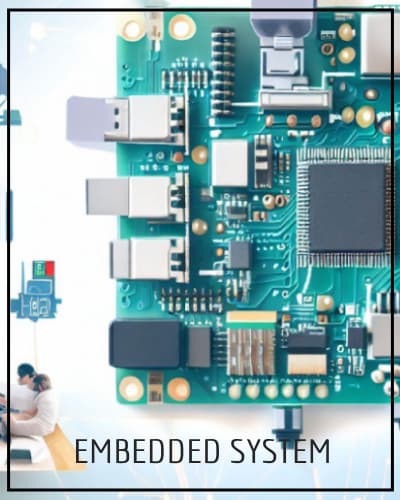
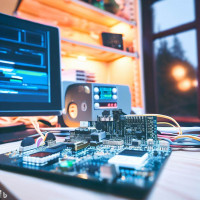
High-density ARM and RISC-V PCB design, multi-layer high-speed differential signal integrity, and thermal simulation management.
Low-level Linux/RTOS driver SDK development, hardware ISP image tuning, microsecond multi-sensor timestamp sync, and Edge AI deployment.
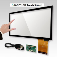
Color bistable electrophoretic ink driver boards, sunlight-readable outdoor digital signage, and custom smart e-label electronics.
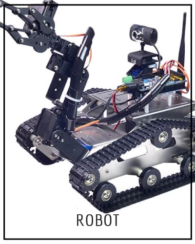
Autonomous navigation vision for AGVs/AMRs, electro-optical gimbal payloads for UAVs, and high-precision industrial inspection equipment.
From initial architecture definition to volume mass production, IADIY eliminates information asymmetry and schedule slippage through disciplined Stage-Gate reviews and tiered issue tracking.

In precision manufacturing and optoelectronic assembly, Manufacturing (MFG) and Quality Assurance (QA) are never adversaries—they are twin engines driving yield ramp-up and long-term reliability. Manufacturing executes disciplined throughput and cycle times, while QA builds data-driven poka-yoke safeguards; locked together, they ensure mass production is both fast and predictable.
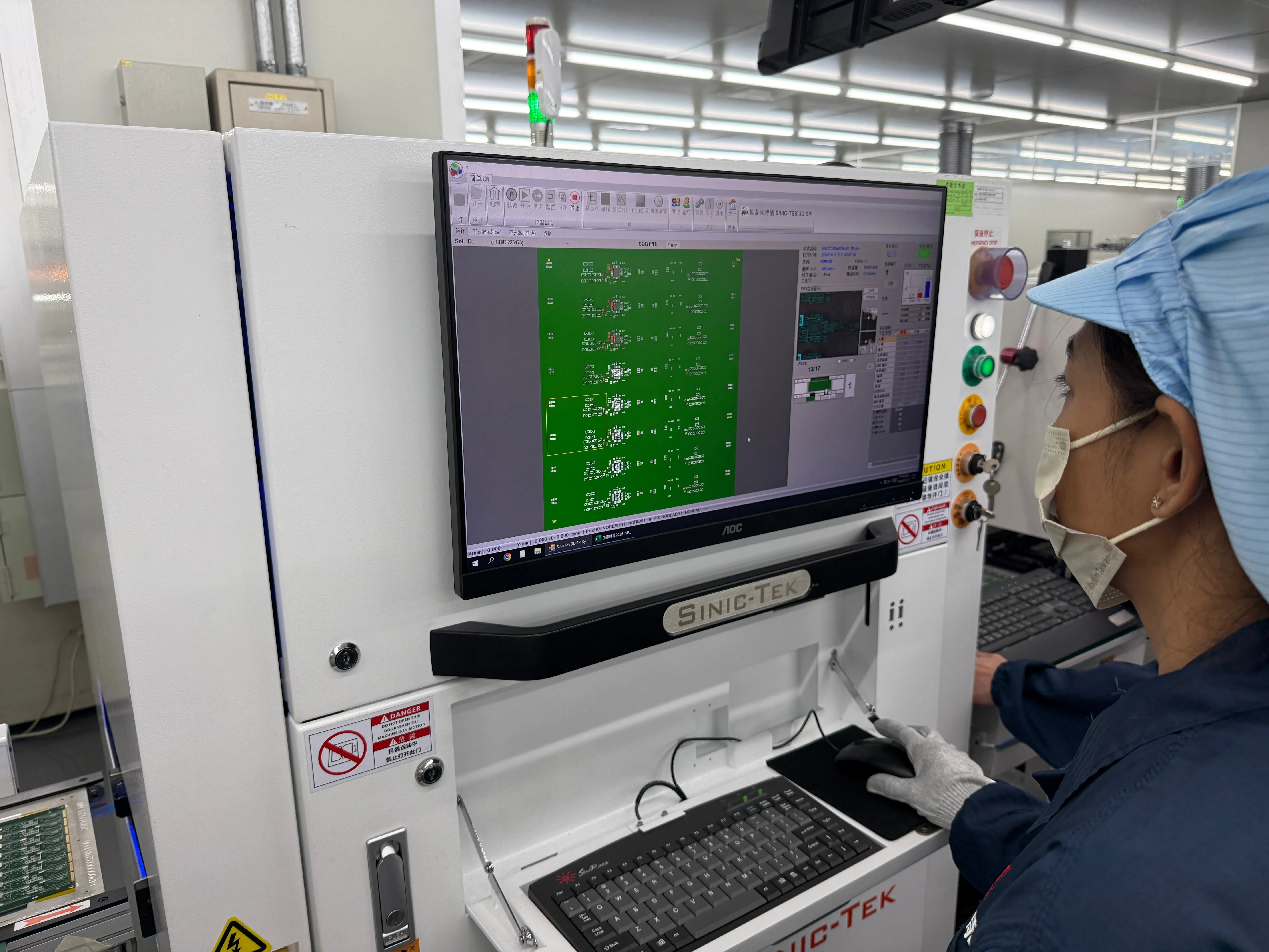
Automated 3D optical measurement of solder paste height, area, and volume—preventing insufficient solder, bridging, and offset at the source.
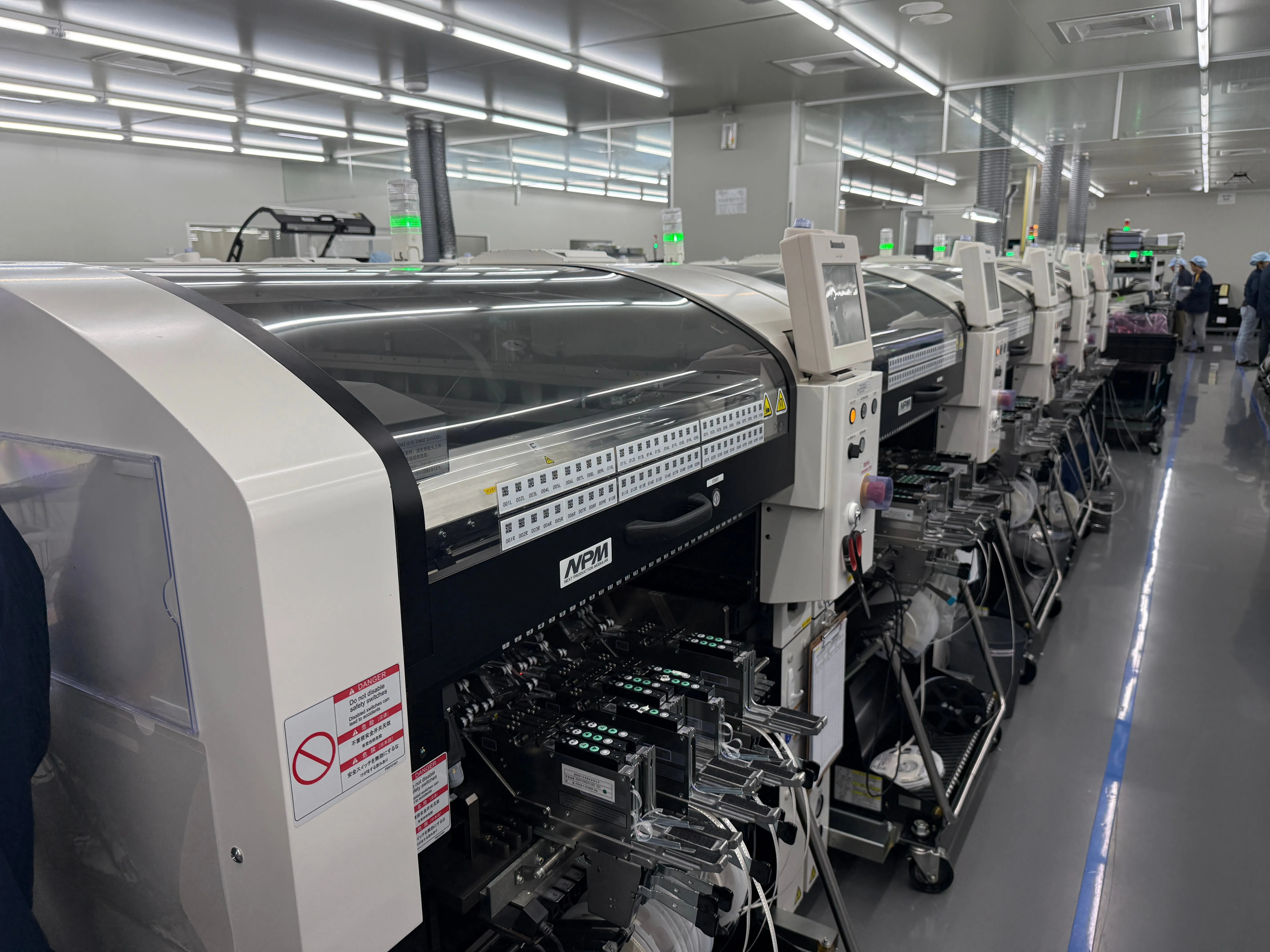
Supports 01005 micro-passives and sensitive optoelectronic components with micron-level vision alignment for zero placement shift.
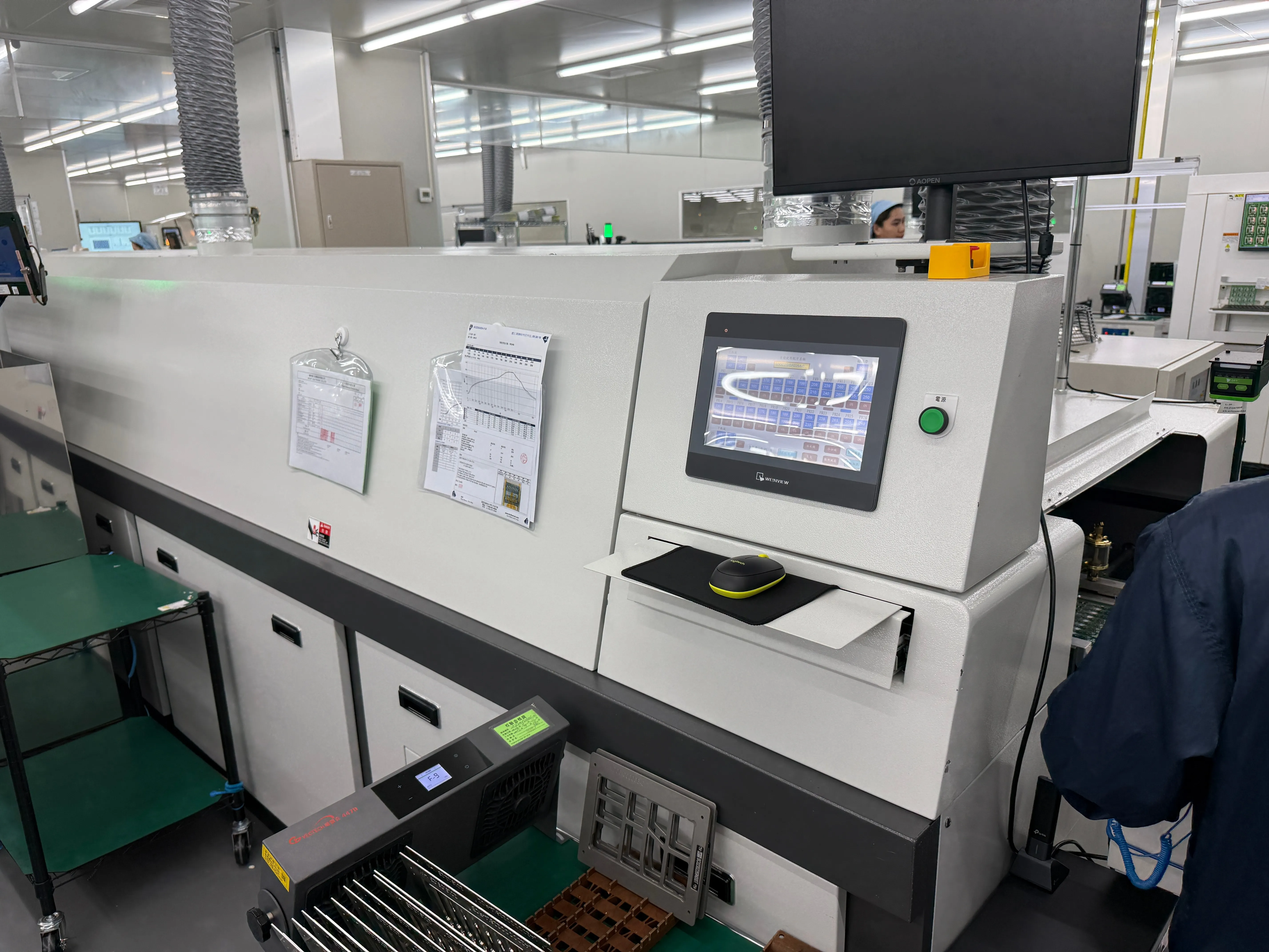
Closed-loop thermal profiling in a low-oxygen atmosphere minimizes solder voids while protecting heat-sensitive optical elements.
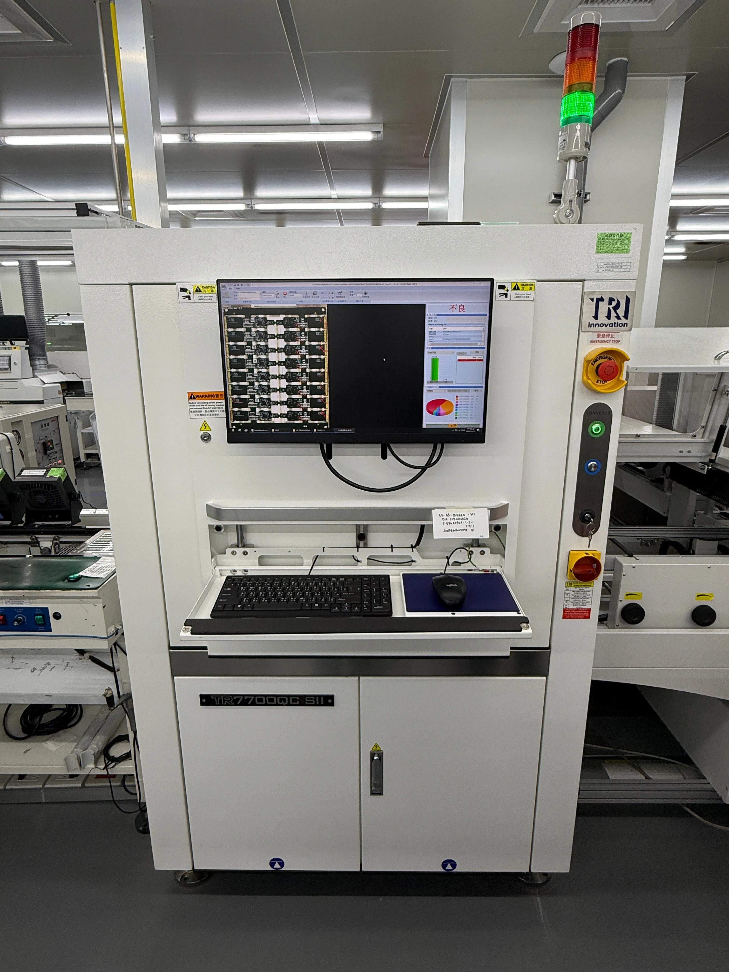
Multi-angle high-resolution optical scanning inspects fillet wetting angles, polarity, and coplanarity—eliminating manual inspection escapes.
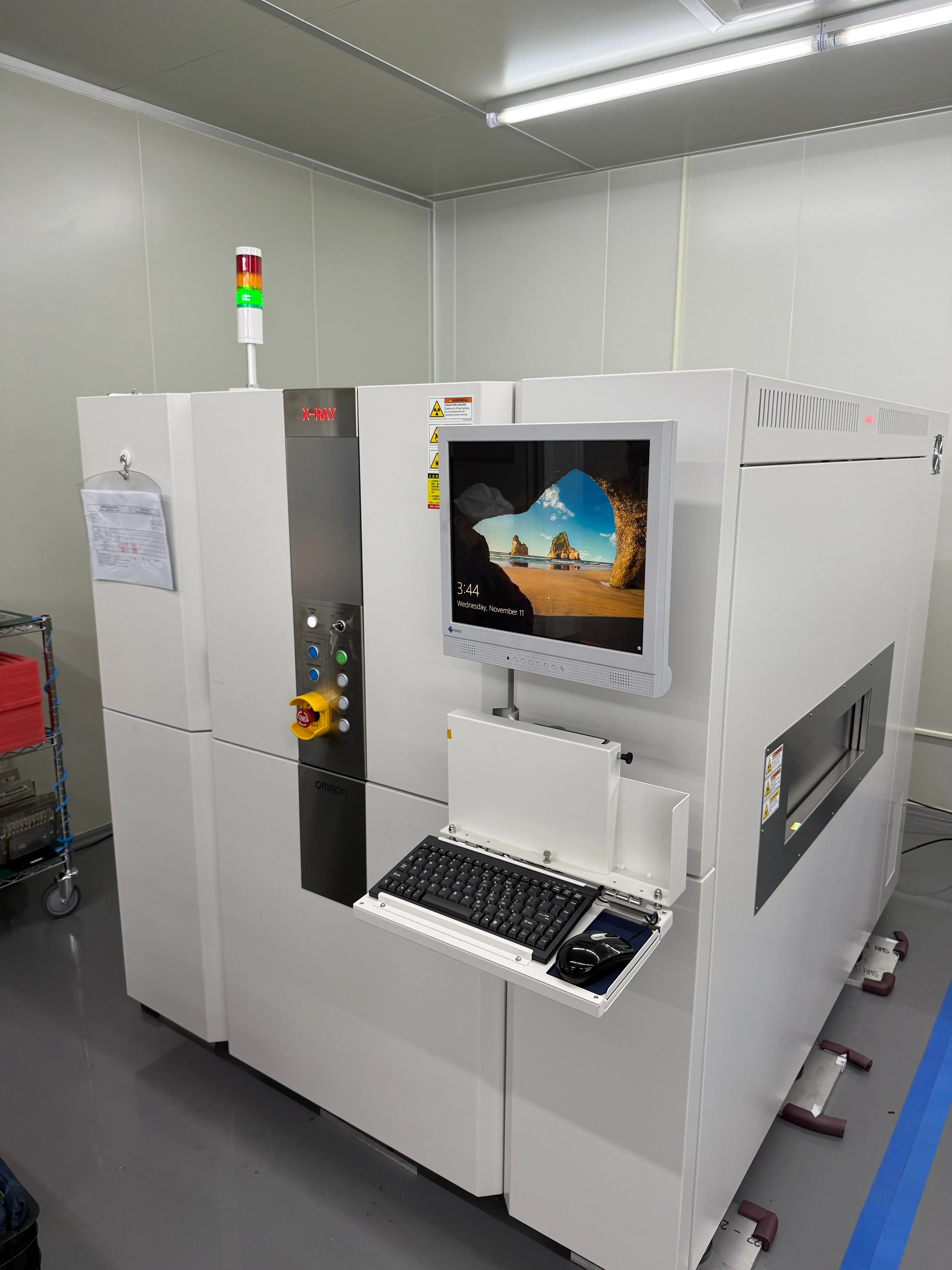
Non-destructive penetration imaging verifies hidden BGA/QFN solder joints and internal package voiding to meet high-reliability standards.
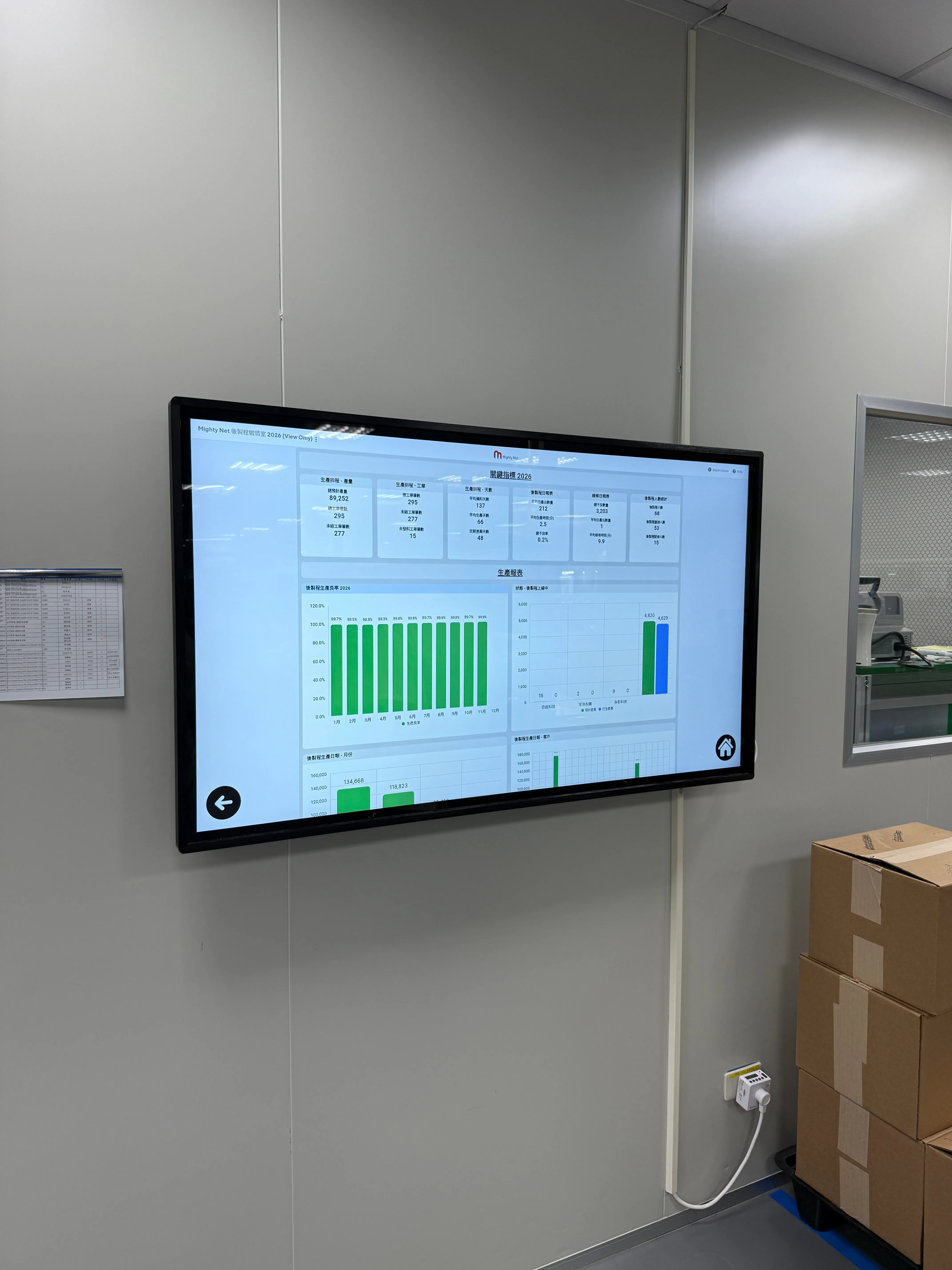
Digital shop-floor dashboards track live yields, process parameters, and 2D unit barcodes—triggering instant alerts with 100% cloud traceability.
Core engineering, optical alignment, and precision assembly are rooted in Taiwan—ensuring zero-lag communication, rapid engineering response, and agile delivery.
Key optical components and core silicon support full BOM origin transparency, meeting stringent US and European cybersecurity and defense procurement standards.
Custom system architectures and developed IP belong 100% to the client, backed by bilateral NDAs and rigorous trade-secret protection protocols.
From precision optical components to turnkey system integration, explore hardware platforms validated in volume production:
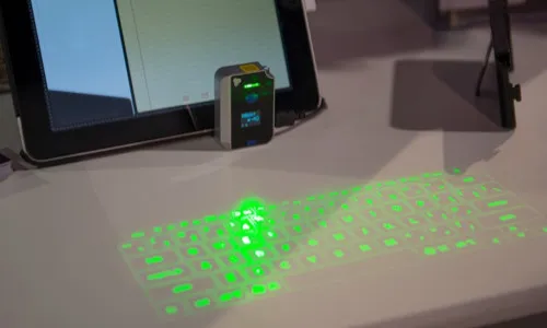
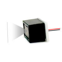
Integrates diffractive optical elements (DOE), IR sensors, and real-time triangulation algorithms to deliver high-immunity input inside a compact cavity.
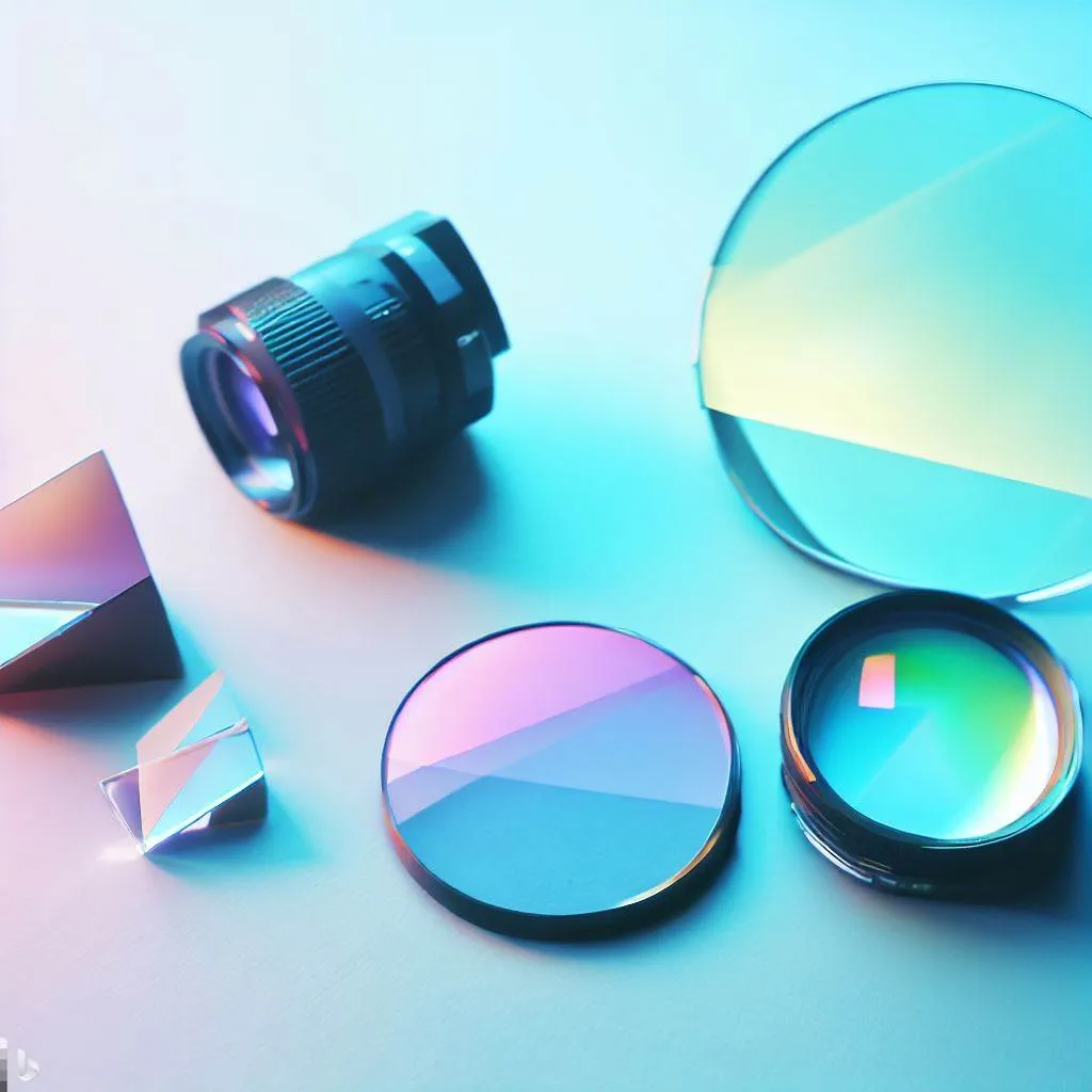
Overcomes high-temperature glass molding bottlenecks to achieve sub-micron surface form accuracy and shock-resistant coatings with zero defocus under heavy recoil.
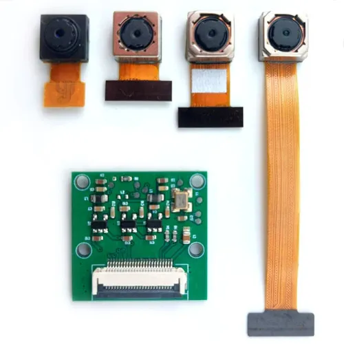
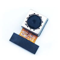
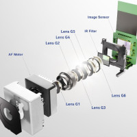
Engineered for space-constrained high-speed imaging—optimizing FPC EMI shielding and active focusing mechanics to significantly cut BOM and assembly costs.
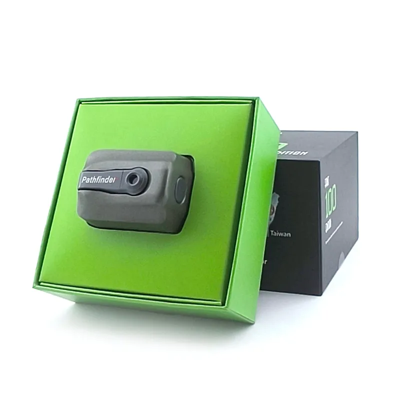
Combines a high-precision optical sensing array with real-time trajectory tracking algorithms to capture clubhead path deviations at impact, demonstrating IADIY's end-to-end JDM capability from sensor selection and mechanical design to embedded software integration.
Field-tested manufacturing insights, thermal management strategies, and global supply chain guides from IADIY senior engineers:
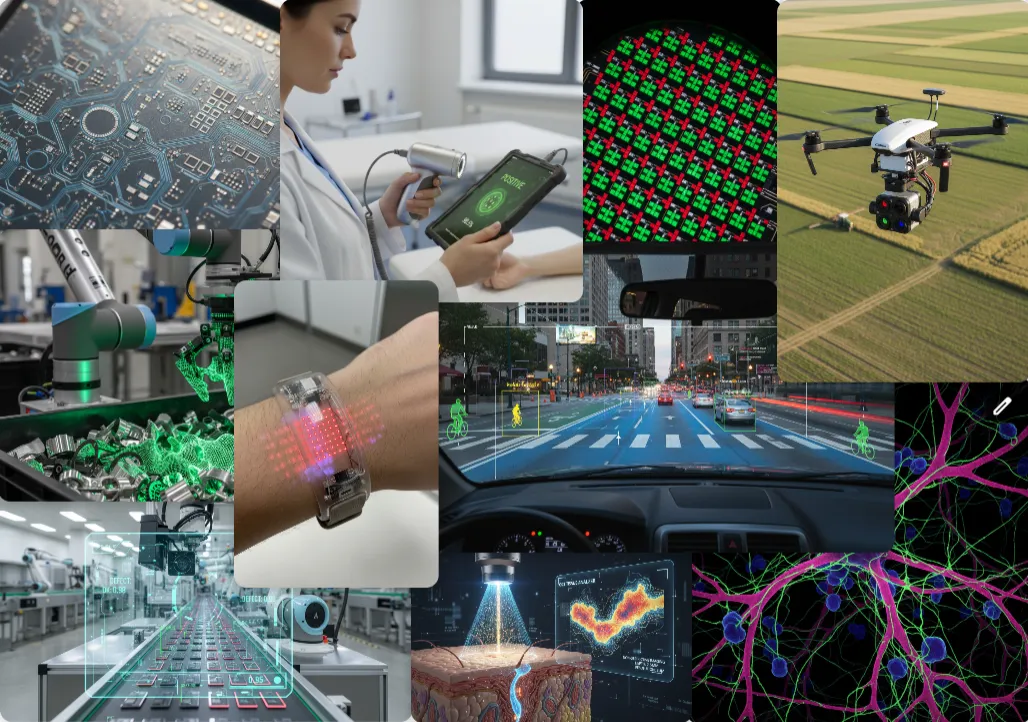
How hardware teams bridge the critical chasm from Proof of Concept (POC) to commercial volume. Combining cross-disciplinary optomechanical R&D, Day-1 DFM, and multi-region manufacturing for predictable, cost-controlled scale...
Spherical lenses offer only a single vertex-curvature degree of freedom, causing spherical aberration at large apertures. Aspherical optics introduce higher-order surface geometry to correct wavefronts and achieve diffraction-limited imaging...
End-to-end optical engineering and contract manufacturing for electro-optical subsystems, complex laser modules, and optical assemblies—backed by in-house optical, IC, and optomechanical teams with strict laser eye-safety compliance...
Tailoring module footprint, lens FOV, auto/fixed-focus actuators, and optical filters across hardware and firmware. Built on IADIY's proven standard camera platforms with structured NRE engineering to cut development time and cost...